Computational semiconductor physics from materials to devices
We develop predictive models and simulation tools to compute the optical, electrical, thermal, quantum, and electromechanical behavior of next-generation semiconductor devices.
Why computational electronics?
Continuing technological advances make possible electronic and photonic devices with increasing structural and conceptual complexity across a widening variety of material systems. Computational electronics combines solid state physics, quantum mechanics, electromagnetics, transport theory, and numerical algorithms to build quantitative descriptions of device operation.
Device structure, material composition, and operating principle are inseparable. Quantum devices can be governed by nanometer-scale coherent transport, heterostructure photonic devices by coupled optical and carrier confinement, and power or wide-bandgap devices by high field and thermal phenomena. The group develops models appropriate to each physical regime and uses them for design and optimization.
Core themes
Semiconductor photonic devices · semiconductor nanoelectronic devices · coupled electrothermal transport · nonlinear phenomena · semiconductor materials and device physics · millimeter-wave and THz sources.
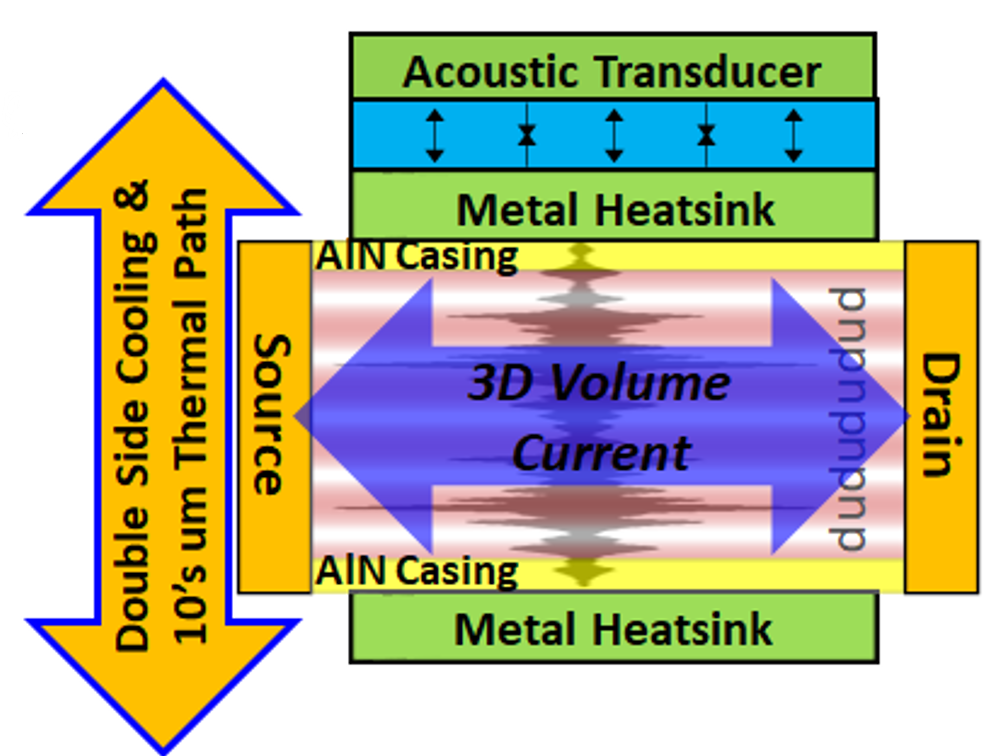
Piezo-acoustic transistors
We are developing quasistatic models for the free and bound interfacial charges in wurtzite III-N epitaxial layer structures as a function of applied compressive stress as a guide to the design of a novel piezo-acoustic transistor. Original time domain models are additionally being developed for longitudinally polarized acoustic waves in wurtzite III-nitride heterostructures. The goal is to connect an externally applied stress waveform to the resulting displacement, strain, piezoelectric polarization, and time dependent interface charge, coupled to fully 2D electrothermal charge transport simulation.
The models explicitly accommodate reflections from device boundaries and are intended to support the design of transistor structures in which mechanical and electronic degrees of freedom are deliberately coupled.
Ultra wide bandgap impurity band transport
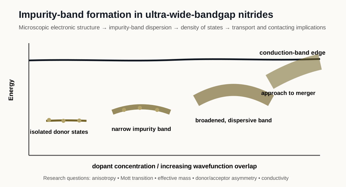
We study how deep dopant states evolve from isolated bound states into dispersive impurity bands as dopant concentration increases, and how that evolution controls conductivity, effective mass, and the approach to the Mott transition.
Recent work established a Green's function framework for donor band formation in AlN. Ongoing work extends the physics toward acceptors, anisotropy, and experimentally relevant transport in ultra wide bandgap materials.
First-principles piezoelectric materials
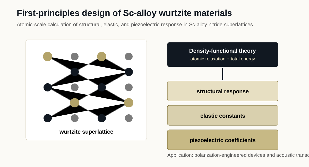
First principles calculations are used to understand how scandium incorporation changes the structural, elastic, and piezoelectric response of wurtzite nitride superlattices. This materials level work provides parameters and physical insight for polarization-engineered acoustic and electronic devices.
GaN traveling-charge-domain sources
Recent work develops a quantitative theory for nucleating traveling charge domains in semiconductors with negative differential drift velocity and identifies diffusion as the microscopic process that suppresses domain formation.
A planar AlGaN/GaN triode architecture provides a route around limitations of conventional bulk Gunn structures. Stochastic Boltzmann transport simulations demonstrate self sustaining Gunn mode oscillation and motivate continued work toward compact millimeter-wave and THz sources.
Sculley & Yoder, 2025
“Nucleation and Propagation of Traveling Charge Domains in a Planar AlGaN/GaN Triode Structure,” physica status solidi (a).